
Scanning force microscopy
(German original "Rasterkraftmikroskopie" by Dipl.-Phys. Karsten Franke - published in DPMA-Erfinderaktivitäten 1998)
This report pertains to the principles of scanning force microscopy and associated technologies which aim at the examination and manipulation of surfaces of all sorts at nanometre scale. Some recent applications in this field filed with the GPTO are briefly presented.
G. Binnig and H. Rohrer developed the so-called scanning tunnelling microscope (STM) at the IBM Zurich Research Lab in 1981/1982, for which they were awarded the Nobel Prize for Physics in 1986. Many other instruments available today for the imaging and manipulation of all kinds of surfaces are based on STM. In STM the sample being investigated is usually not destroyed. This technique produces high-resolution images of the topography of samples while allowing to selectively study their physical properties.
STM and other scanning microscopy techniques can be used under normal atmospheric conditions, in contrast to, for instance, electron microscopy. To study and obtain images of structures at the atomic scale, electron microscopy requires sophisticated sample preparation techniques and high vacuums, while the samples usually suffer damage.
The STM scans an extremely fine sharpened metal tip, line by line, over the sample surface at a distance of a few nanometres, using piezoelectric transducers. The surface has to be conductive. A small voltage is applied between the tip and the surface, and a tunnelling current which flows between the gap is measured and fed into an electronic feedback control circuit. The strength of the tunnelling current depends on the distance between the surface and the tip. The feedback signal controls another piezoelectric transducer that changes the z distance between the tip and the surface. If the tunnelling current is kept constant, hence maintaining the distance, the tip will trace the topography of the surface. Combined with the information on the respective x- and y-coordinates of the tip (scanning the surface), this gives a three-dimensional image of the sample surface with a resolution on the order of tenths of nanometres (horizontally 0.1 nm, vertically down to 0.01 nm) which is displayed on a screen.
While this basic method was still limited to investigations of conductive samples, the later development of the so-called atomic force microscope AFM (or SFM scanning force microscope - in 1985, first, by G. Binnig and C. F. Quate) and its successors allowed to study insulating and semi-conducting samples. In this technique a fine sharpened tip, ideally having a single atom at the apex, scans a sample surface in very close proximity, the so-called near-field technique. Interatomic forces act between the tip, usually mounted on a cantilever (spring lever arm) and the respective nearest sample surface atoms. The sample can be investigated in the contact mode, the intermittent contact mode and the non-contact mode.
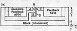
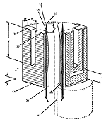
In the contact mode the overlapping electron clouds of the atoms create extremely short-range repulsive forces. To maintain these locally very strong forces constant, and therefore also the distance between the tip and the sample - as a basis for obtaining a topographic map of the sample surface in analogy to the STM method - the z movement of the tip has to be measured. This was at first achieved by using an additional downstream STM, where the sample surface of conventional STM investigations is replaced by the back of the conductive cantilever (cf. Fig. 1 - according to Ch. Bai, Scanning Tunneling Microscopy and its Application, Springer Series in Surface Sciences 32, Springer-Verlag, 1992). Later techniques directly measure the deflection of the cantilever interferometrically or capacitively, or e.g. by using a laser (Fig. 2 - DE 19504855 A1). Today, piezoelectric elements (cf. Fig. 6 and 7) are used for measuring deflection. The piezoelectric elements are often directly mounted on the cantilever or - in the non-contact mode - on the oscillator, and respond to the bending of the cantilever. However, contact mode investigation may lead to damage of the sample surface and wear of the tip, causing lower resolution, in particular.
In the non-contact mode, which naturally causes no damage at all, the tip of a modified AFM is merely close to the sample without contacting it. This allows for example to study soft materials, e.g. biological samples. In this mode, the tip of the microscope oscillates - driven by a piezoelectric transducer - close to its resonant frequency. As the oscillating tip approaches the sample surface, weak short-range attractive forces act between the tip and the sample, the so-called van der Waals forces. The effect of van der Waals forces may be intensified on the sample surface by the surface energy of gas and liquid adsorbates (e.g. hydrocarbon molecules, water vapour or condensation water from the ambient air). The attractive forces manifest themselves in a reduction of the resonant frequency and of the oscillation amplitude of the microscope tip. A laser interferometric technique, for example, allows to measure the oscillation amplitude. If the feedback circuit maintains the oscillation amplitude constant, which corresponds to constant distance and constant force, a topographic image of the sample can be generated in analogy to the above mentioned microscopy techniques. However, the local resolution in the non-contact mode is often very limited, particularly when used in ambient atmosphere, due to the impact of the adsorbate layers on the damping of the oscillation of the microscope tip leading to the distortion of the topography information.
The intermittent AFM operation mode has become important in practice. In intermittent mode the oscillation amplitude of the probe tip is much larger than in non-contact mode. When the tip comes close to the sample surface, the interactive forces dampen oscillation, reduce the amplitude and the tip makes contact with the sample surface many times and very slightly for each measurement point (the so-called tapping mode). The energy turnover of the tapping mode is essentially reduced compared to the contact mode allowing to study also sensitive samples easily prone to suffer damage, like biological materials or semi-conductor wafers. The lower oscillation amplitude resulting from damping is maintained constant through an electric feedback loop so that the central z-coordinate of the tip follows the sample topography.
Special designs of the microscope tips and the scanning processes in the AFM non-contact mode or tapping mode enable the study of e.g. the magnetic and electrical properties of sample surfaces. For example, the magnetic microscope tip of a MFM (magnetic force microscope) can measure the storage density or storage quality of magnetic storage media. Electrical properties of surfaces, e.g. the concentration and distribution of dopants in wafers, which are critical parameters of microchip production, can be measured by EFM (electrostatic force microscopy). The data is collected during a single scan of the sample surface, in two separate passes for each measuring point. In the first pass, the atomic interactions between the sample and the oscillating tip are detected to record the topography data of the sample (preferably in the tapping mode). In the second pass, the data on magnetic or electrostatic interactions are generated, taking into consideration the sample topography, recorded immediately before, during the first pass. In the second pass, the distance between tip and sample is increased (lift mode) so that the impact of atomic forces is negligible since atomic forces are significantly shorter-ranged than electric or magnetic forces.
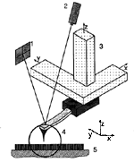
Another AFM technique is the Nearfield Scanning Optical Microscopy (NSOM). NSOM can be used in combination with AFM or its derivatives: For example, an optical fibre may be used for the AFM tip. In this NSOM technique, the tip is raster scanned point by point across the sample. The optical fibre tip has an opaque coating at the end except for an aperture in the subnanometre range (compare Fig. 3 - loc. cit. Bai) through which laser light is emitted, illuminating or transmitting the sample. The light interacting with the sample is collected by a position-sensitive detector - e.g. in the transmission mode, the reflection mode or the fluorescence mode - building up a raster image of the sample surface in close proximity to the aperture. In NSOM resolution of the image is not limited by diffraction.
Surface modification
The effectiveness of the above instruments for high-resolution imaging of surfaces and for providing pictures of objects whose size is on the scale of atomic diameters, also suggest their use for controlled chemical or physical modifications of surfaces on the nanometre scale. STM for example offers controlled manipulation of metal surfaces by direct mechanical impact of the microscope tip. When a current is applied at the tunnelling gap, it is possible to move atoms out of the crystal lattice into other positions of the sample surface, to segregate material from the tip itself depositing it on the sample or to remove material using etching techniques, likewise it is possible to perform a variety of chemical surface reactions and to deposit metal (e.g. as circuit tracks) extracted from gas compositions. STM can also be used to locally expose preferably ultrathin electron resist layers in analogy to electron beam lithographic processes. In this case, the STM may be operated in the field emission mode. The applications of surface manipulation on the nanometre scale include, for example, the repair of integrated circuits or masks for conventional electron beam lithography.
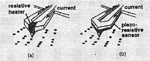
The AFM can be used for surface modifications of semiconducting or electrically insulating materials, usually working in the contact mode. Soft materials, for example, ultrathin resist layers for lithographic processes can be mechanically scribed and removed. A silicon cantilever with integrated resistance heating and piezoresistive sensor can heat the AFM tip to a maximum temperature of 170°Celsius. Local melting processes will allow to thermomechanically integrate structures, e.g. into plastics, such as PMMA (polymethylmethacrylate), for storing and reading digital information (cf. Fig. 4 - according to B.W. Chui, J. Microelectromech. Syst. 7, 1998, 69). At IBM this method has been used to achieve storage densities of 1,010 bits/cm2 - i.e. roughly 25 times the storage capacity of modern hard disks.
Another future oriented application of the nanomodification of objects using the AFM concerns biological materials, such as DNA molecules which can be imaged and manipulated simultaneously; for instance, the strands may be separated at predefined places with utmost precision, for example, to cut out defective gene sequences, which are later replaced by modified DNA fragments.
Recent DE patent applications on AFM
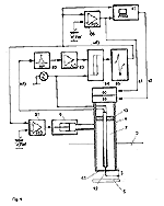
Technical solutions of recent applications filed at the GPTO relate to the design of the units controlling the oscillation of the microscope tip and the analysis of the oscillation variations caused by the impact of the above mentioned forces. DE 19510368A1 (cf. Fig. 5) proposes the use of a coupled oscillator arrangement, specifically a tuning fork (but compare also K. Dransfeld, EP 0372060 A1) to which an optical fibre is attached that can be utilised as AFM probe or NSOM probe. The oscillator surface is of multi-layer piezoelectric materials which can stimulate and maintain oscillation (actuator layers), while simultaneously recording the variations in oscillation (detector layers).
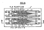
Several solutions were suggested for combining the modes of operation of AFM, STM and NSOM in one instrument: one of these solutions, presented in DE19531466A1, suggests the use of a multi-layer cantilever arrangement - consisting of a layer of piezoelectric material for scanning or stimulating the oscillator to perform the AFM function (contact mode and non-contact mode) as well as several metallic layers and an optical fibre layer to fulfil the STM or NSOM function - with a optically transparent probe tip at the end (cf. Fig. 6). Related solutions, i.e. instruments combining several modes of operation, are described in two other applications: DE 19513529A1 (AFM/STM) and DE19713746A1 (AFM/NSOM).
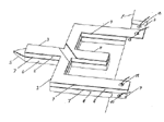
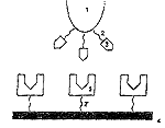
For faster reading and writing speeds of data memories, operating on the above thermo-mechanical principle, arrays of cantilevers with AFM tips were designed to simultaneously read and write a large number of bits. DE 19701701A1 describes an array where the individual probes are arranged in a V-shape to form a mutually nested arrangement of probes and to achieve a high density of probes (cf. Figure 7).
In DE 19700747A1, a scanning force microscopic probe, consisting of the basic probe body, a piezoelectric resonator and a probe tip, is used for investigations in liquid. The probe is arranged in a gas-filled capillary tube: the open end of the tube pointing to the object being measured, and the probe tip protruding from the tube. The pressure of the gas in the capillary tube is maintained so high that no liquid or hardly any liquid can enter the capillary tube thus avoiding falsification of the cantilever oscillation (Figure 8).
DE 19631326A1 describes a method for measuring specific interactions between different molecular or biological species produced due to bonding forces, using scanning force microscopy. The interactions are macroscopically related to the properties of active compounds. A defined minuscule amount of a species (of the active compound) being tested is fixed to the AFM tip while material of a second receptor compound (possibly reacting to the first compound) is bound to macromolecules, for example (quasi functioning as an object slide). Measuring the forces effective between the active compounds in a reproducible manner using SFM allows to draw conclusions about the properties of the active compounds of the system being investigated. This is an effective method for screening a large number of combinations of substances (Fig. 9) to be utilised as specific active compounds.
Another application (DE 19531068A1) relates to a method for mask production on a semiconductor substrate. The mask consists of an electron beam resist (preferably, PMMA) which is partly removed under the action of a fluid (preferably, a composition of methylisobutyl ketone and isopropanol) and under the action of a force acting between the moving probe tip of a scanning force microscope and the mask surface.
References:
- Ch. Bai: Scanning Tunneling Microscopy and its Application, Springer Series in Surface Sciences 32, Springer-Verlag, 1992
- B.W. Chui: J. Microelectromech. Syst. 7, 1998, 69
![]()
Fig. 1: original AFM
(compare Ch. Bai, 1992)
![]()
Fig. 2: Force microscope measuring the deflection of the cantilever using a laser beam
(published patent application DE 19504855A1)
![]()
Fig. 3: NSOM technique
(compare Ch. Bai, 1992)
![]()
Fig. 4: Thermomechanical storage of data using AFM with a cantilever that has an integrated heating device to store information and a piezoelectric sensor to read information
(compare B.W. Chui, 1998)
![]()
Fig. 5: Oscillator arrangement with a glued-on optical fibre for combined AFM/ NSOM with piezoelectric material with a detector function and an actuator function
(published patent application DE 19510368A1)
![]()
Fig. 6: Multi-layer cantilever arrangement for AFM/STM/NSOM combination
(published patent application DE 19531466A1)
![]()
Fig. 7: Nested arrangement of an array of AFM probes
(published patent application DE 19701701A1)
![]()
Fig. 8:
(published patent application DE 19700747A1)
![]()
Fig. 9: Screening of active compounds using scanning force microscopy
(published patent application DE 19631326A1)
Copyright © Deutsches Patent- und Markenamt 2004