
Milestones of Relay Development
(German original "Meilensteine der Relaisentwicklung" by Dipl.-Ing. Werner Kirscheneder, published in DPMA-Erfinderaktivitäten 1999)
The article describes generation leaps that occurred in the development of electromechanical relays, by the examples of R-relays (SAUER / MATSUSHITA) and silicon micro relays (SIEMENS).
From time to time, any technological field is revolutionised by a pioneering achievement. The big brainwave is followed by many small steps consisting of variants and embodiments of the basic idea so that the whole field eventually reaches a higher technological level. As a rule, many years will pass until the achieved state is again set in motion by a new pioneering achievement.
The era of electromechanical relays seemed to have come to an end in the 1960s. Transistors were widely introduced at a fast pace and built into almost any electric device. They were much smaller than the formerly used electron tubes, which they largely replaced. Furthermore, they were more reliable, had a nearly unlimited service life and were easy to insert into printed circuit boards. Conventional electromechanical relays simply did not fit with this new technology because of their size and high power consumption [1]. And almost anybody assumed that transistors would replace relays, in particular with circuit boards. The necessity of full electrical isolation and smaller size along with a reduction of the actuating force eventually generated a new upswing in relay technology.
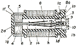
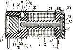
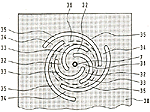
German patent specification DE-PS 1243271 of the year 1966 describes an electromechanical relay in the form of a reed switch relay (Fig. 1) that complies with modern switching technology due to its small size and low power consumption.
Instead of a conventional reed glass-tube contact, a ferromagnetic contact stud is directly provided in a coil body designed as a protective tube. Pole shoes of a permanent magnet provided in the coil body flange are at the same time used as permanent contacts. The obtained type R relay features, above all, a compact design. Its volume is only 2 cm3, which is about one tenth of the customary volume of comparable earlier models [2].
At the same time, the superposition of the fluxes of the permanent magnet and of the actuator magnet in the contact air gap provides for a high responsiveness and low operate power consumption. A highly efficient polarised relay had thus been developed with little effort. Due to the small mass of moving parts - the only part being the contact stud forming the armature - switching frequencies of up to approximately 1 kHz were obtained.
The low power consumption was related to weak self-heating. This allowed for a high packing density for applications on printed circuit boards. The properties of the R relay met virtually any requirement of the new switching technology. On the occasion of the "electronica 1968" fair, the R relay was attributed an award for its high technological standard. And everybody using the first German key telephone heard its gentle clicking noise [4].
This novel concept was further improved in the course of the following years to enhance production, quality and application of the R relay.
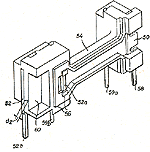
Patent of addition DE-PS 1909940 (Fig. 3) shows the concept of a coil body determining the relay design, designed for series production. Contact elements and pole shoes of a specific shape are firmly embedded in plastic parts. A chamber is provided in the coil body flange for receiving a ceramic non-conductive permanent magnet made of BaOFe [5]. A monostable or bistable switching behaviour is easily achieved by selecting appropriate distances of the permanent magnet and the opposite pole shoes. The ceramic magnet has a negative temperature coefficient which largely compensates that of the coil and thus considerably extends the application range of the relay.
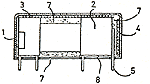
Patent DE 2353444B2 (Fig. 4) describes how the R relay is embedded in insulating material in order to seal the contact chamber for providing protection against environmental influences, which is very important for the reliability of the relay.
For further enhancing contact reliability of the R relay, DE 2462277C3 (Fig. 5) describes the possibility to activate the ceramic permanent magnet as getter. For this purpose, the permanent magnet is activated by means of a pre-treatment in order to bind long-term contact damaging substances in the contact chamber and avoid that these substances condense on the contacts and impair the contact resistance. Application of this process will increase life by 10 to 40 times and contact reliability by more the 100 times, depending on the individual case [3].
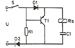
Patent specification DE 2747607C3 describes a relay control arrangement (Fig. 6) allowing to benefit from the advantages of bistable R relays for monostable switching, too. These advantages are the following: low energising power, unnecessary warming-up avoided, low thermal tension, increased reliability even of neighbouring components and temperature compensation of the excitation voltage.
A bistable relay RIs is energised by the charging current of the capacitor and switches when an excitation voltage U is applied. There is no further flow of current due to the charge of capacitor C1 - yet the relay remains in its activated position because of its bistable character. For switching back by removing the excitation voltage U, capacitor C1 is short-circuited through the semiconductor route T1, switched in parallel to the relay. Relay R1s is inversely energised and reverts to its deactivated position, like a monostable relay. This allows to energise the R relay with minimum control power. Due to its simple design, this circuit could be integrated into the R relay [6], as shown by an application within the scope of a space mission.
Due to the properties described, advantageous for modern switching technology, R relays were of particular commercial importance. Several hundred million of these relays were utilised in the course of more than 30 years.
This example shows that it may be sensible not to abandon an apparently technologically exhausted component, such as the electromechanical relay, and to pursue its development despite spectacular innovations in other fields such as semiconductors.
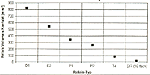
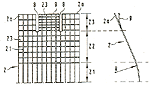
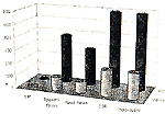
Innovations and improvements have repeatedly allowed to reduce the volume and the wafer size of conventional electromechanical relays by up to 50%, when passing from one generation to the next. Fig. 7 provides a comparison of sizes (volume/contact travel) of the following relay generations produced by Siemens: small relay D1 (1 change-over contact) (DE 2701230C3, DE 2723219C2, DE 2723220C2); small relay D2 (2 change-over contacts) (DE3132239C3); mini relay P1 (1 change-over contact) (DE 3338198A1); mini relay P2 (2 change-over contacts) (DE 4309618A1); telecom relay T4 (2 change-over contacts) (applications DE 19850667 and DE 19850668); and silicon micro relay SIR (16 closers) (DE 4205029C1) [7]. The impressive number of patent applications is proof of the know-how, growing with the miniaturisation of relays.
Apart from stable low costs, this explains why electromechanical relays, despite prophecies of doom, have not only remained on the market but have even shown rising sales figures. This applies to both small signal/telecom relays and power relays for industrial and automotive electronics.
Miniaturisation does, however, affect control and load specifics of relays. Technical specifications tend to become more stringent. Small signal/telecom relays in particular are being pushed to their physical limits in terms of coil wire thickness, size and precision of injection mouldings, or complexity of production lines. It has become increasingly difficult to put ever smaller relays on the market at reasonable cost [8].
The silicon micro relay, whose development has allowed to perform a quantum leap in both control and miniaturisation, presents a way out of the dilemma. Conventional design and production methods of relays are being put aside, since this relay is based on MEMS (Micro-Electro-Mechanical Systems) technology. This novel component combines the benefits of conventional relays (eg. full electric isolation, robust design, low contact resistance) and semiconductor switches (eg. standardisation, small size, low operate power consumption) [8].
The mode of actuation is the key design parameter of silicon micro relays. Since, in electromechanical relay actuation, the volume and the manufacturing costs are largely determined by the coil, whose size can hardly be further reduced, research focused at an early stage on developing alternative modes for actuating relays. It was important to find a suitable compromise between power consumption, contact force and thus contact reliability, and size. It was found, on the one hand, that it was impossible to obtain performances below 100 mW with sufficient contact force using planar coils or thermal actuators; on the other hand, even Piezo actuators or other switching principles did not yield satisfactory results with regard to the possible volume or the switching characteristics.
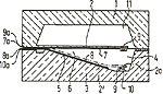
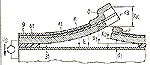
Electrostatic actuation, too, had been explored again and again, without leading to marketable products. Finally, a technological and commercial breakthrough was achieved by the development of the so-called moving wedge concept (DE4205029C1) (Fig. 8), working as follows: A spring leaf etched out of silicon and a counter plate form a wedge-shaped air gap. If a voltage is applied between the counter plate and the spring leaf, the latter unrolls on the counter plate. Starting at the narrowest spot of the air gap, where the spring leaf is fixed and where the electrostatic forces of attraction are highest, the unrolling movement is pursued to the free end of the spring leaf. A contact is closed at this free end of the spring leaf. Contrary to conventional designs, the electrostatic actuation does not have to overcome a large initial distance of electrodes; rather, important electrostatic forces occur at the respective most inward spot of the air gap, and move further on to the free end when the spring leaf is being closed (moving wedge concept) [9].
Silicon micro relays are largely produced using the process technique applied in semiconductor manufacturing. For example, the spring leaf, which is 1 mm to 1.5 mm long and 0.5 mm wide, is etched out of a silicon substrate. The individually doped layers provide for a predetermined bending of the spring leaf. Further structuring enhances the switching characteristics of the relay. In DE 4437259C1, the contact force of the spring leaf is increased (Fig. 9). DE 4437260C1 describes how to avoid transverse bulging of the spring leaf by providing slots (Fig. 10). Under DE 4437261C1, crawling contact making is avoided by a geometric discontinuity of the air gap. DE 19736674C1 describes an overlapping of movable contact and static contact (Fig. 11). Manufacturing in MEMS technology allows, in addition, to produce multiple switches (up to 16) in a single package and to integrate additional logic elements.
According to a market survey [9], the silicon micro relay is not only suitable for applications of conventional electromagnetic relays but also for those of small signal switching components such as semiconductor relays and optocouplers. It is an interesting solution for applications "requiring
- full electrical isolation
- linear transfer characteristic
- low and stable contact resistance
- extremely short switching times
- low operate power consumption
- standard IC packages
- multiple switches in one package." [8]
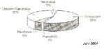
Possible applications do not only cover the field of telecommunications but also automotive electronics, consumer electronics, medical engineering, instrumentation and control and security systems. [9] shows how the silicon relay is expected to establish itself on the market, among the known small signal switching components (with full electronic isolation) (Fig. 12). The advantages over the latter regarding power loss are also presented in [9] (Fig. 13).
The described electromechanical relays show in an impressive way how inventive minds find new ways to drive innovation, even relating to components, such as relays, whose technological development seemed to have come to an end.
References - "Relay technology"
- Brillante; Electronics Journal; 1974
- SAUER, Hans: Die Effizienz von Relais und deren wirtschaftliche Bedeutung; Bauelemente der Elektrotechnik; 1976
- SAUER, Hans: Preiswerte Relais - um Größenordnungen zuverlässiger; Elektronik; 1976
- SAUER, Hans: Reedrelais auf alten und neuen Wegen; etz; 1979
- WEBER, Dr., Ernst: Zuverlässig schalten; Elektronikpraxis; 1981
- ANTONITSCH, Sepp: Bessere Relais-Eigenschaften durch integrierte C-Schaltung; und-oder-nor + Steuerungstechnik; 1983
- Siemens: Datenbuch Relais; 1992
- MATTIUZZO, Ricardo: Silicon micro relay in MEMS technology, The best of both worlds; Components; 3/99
- MATTIUZZO, Ricardo: Technologie-Symbiose; F & M; Jahrg. 107(1999)631
![]()
Fig. 1: DE-PS 1243271
![]()
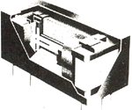
Fig. 2: R relay
![]()
Fig. 3: DE 1909940
![]()
Fig. 4: DE 2353444B2
![]()
Fig. 5: DE 2462277C3
![]()
Fig. 6: DE 2747607C3
![]()
Fig. 7
![]()
![]()
Fig. 9: DE 4437259C1
![]()
Fig. 10: DE 4437260C1
![]()
Fig. 11: DE 19736674C1
![]()
Fig. 12: Market shares according to Mattiuzzo [9]
![]()
Fig. 13: Power loss according to Mattiuzzo [9]
Copyright © Deutsches Patent- und Markenamt 2004